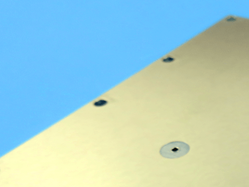
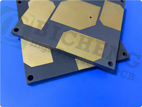
Wangling F4BTMS615 2-Layer 0.254mm Immersion Tin PCB for Aerospace Applications1.Introduction to Core Technologies The F4BTMS series is an upgraded version of the F4BTM series. It has achieved a technological breakthrough in material formulation and manufacturing processes. The material has been enriched with a significant amount of ceramics and reinforced with ultra-thin and ultra-fine glass fiber cloth, resulting in substantial improvements in material performance and a broader range of dielectric constants. It is a high-reliability material suitable for aerospace applications and can replace similar foreign products. By incorporating a small amount of ultra-thin and ultra-fine glass fiber cloth and a large amount of uniformly distributed special nano-ceramics mixed with polytetrafluoroethylene resin, the negative effects of glass fiber on electromagnetic wave propagation are minimized. This reduces dielectric loss, enhances dimensional stability, and decreases the X/Y/Z anisotropy of the material. It also increases the usable frequency range, improves electrical strength, and enhances thermal conductivity. Additionally, the material exhibits excellent low thermal expansion coefficient and stable dielectric temperature characteristics. The F4BTMS series comes with RTF low roughness copper foil as a standard feature, which reduces conductor loss and provides excellent peel strength. It can be used with either copper or aluminum bases. 2.Key Performance Characteristics: Dielectric constant (Dk) of 6.15 at 10GHz 3.PCB Details
4.PCB Stackup (2-Layer Rigid Structure) Copper Layer 1 - 35 μm 5.PCB Statistics Components: 18 6.Typical Applications Aerospace equipment, space and cabin equipment 7. Quality Assurance Artwork Format: Gerber RS-274-X |
Get a Quick Quote
Fill in the form below and our engineers will reply within 24 hours with technical specifications and pricing for Wangling F4BTMS615 2-Layer 0.254mm PCB.
.jpg)
.jpg)

